EXCELLENCE IN INNOVATIVE OPTICAL SYSTEMS
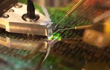
The photonics platform is France’s largest R&D center for the development, characterization, and simulation of optoelectronic systems and components. The platform’s activities range from system and component design through to component fabrication, integration into systems, and packaging and cover III–V and II–VI semiconductor technologies. The technologies developed can be applied to lighting, microdisplays, optical transmission, visible and IR imaging, astrophysics systems, and more. The platform is home to 1,500 sq. m of characterization facilities, 300 sq. m of packaging labs, 1,500 sq. m of materials research space, and 900 sq. m of clean rooms dedicated to III–V and II–VI semiconductor technologies. These resources round out the equipment available at the 300 mm nanoelectronics platform and the 200 mm and 300 mm microsystems platform. With a staff of 300, more than 300 instruments and machines, a broad scope of R&D, and high-quality research results (60 patents filed per year), the platform is the R&D partner of choice of more than 40 companies, including STMicroelectronics, Alcatel-Lucent, Thales (via III–V Lab), Sofradir, Aledia, MicroOLED, and others.
> Access to: All TECHNOLOGY PLATFORMS
OUR Technologies

ALL TECHNOLOGIES